Tuesday, June 13, 2017

JuST FOR THE KNOWLEDGE

JuST FOR THE KNOWLEDGE*

1. *PAN* - permanent account number.
2. *PDF* - portable document format.
3. *SIM* - Subscriber Identity Module.
4. *ATM* - Automated Teller machine.
5. *IFSC* - Indian Financial System Code.
6. *FSSAI(Fssai)* - Food Safety & Standards Authority of India.
7. *Wi-Fi* - Wireless fidelity.
8. *GOOGLE* - Global Organization Of Oriented Group Language Of Earth.
9. *YAHOO* - Yet Another Hierarchical Officious Oracle.
10. *WINDOW* - Wide Interactive Network Development for Office work Solution.
11. *COMPUTER* - Common Oriented Machine. Particularly United and used under Technical and Educational Research.
12. *VIRUS* - Vital Information Resources Under Siege.
13. *UMTS* - Universal Mobile Telecommunicati ons System.
14. *AMOLED* - Active-matrix organic light-emitting diode.
15. *OLED* - Organic light-emitting diode.
16. *IMEI* - International Mobile Equipment Identity.
17. *ESN* - Electronic Serial Number.
18. *UPS* - Uninterruptible power supply.
19. *HDMI* - High-Definition Multimedia Interface.
20. *VPN* - Virtual private network.
21. *APN* - Access Point Name.
22. *LED* - Light emitting diode.
23. *DLNA* - Digital Living Network Alliance.
24. *RAM* - Random access memory.
25. *ROM* - Read only memory.
26. *VGA* - Video Graphics Array.
27. *QVGA* - Quarter Video Graphics Array.
28. *WVGA* - Wide video graphics array.
29. *WXGA* - Widescreen Extended Graphics Array.
30. *USB* - Universal serial Bus.
31. *WLAN* - Wireless Local Area Network.
32. *PPI* - Pixels Per Inch.
33. *LCD* - Liquid Crystal Display.
34. *HSDPA* - High speed down-link packet access.
35. *HSUPA* - High-Speed Uplink Packet Access.
36. *HSPA* - High Speed Packet Access.
37. *GPRS* - General Packet Radio Service.
38. *EDGE* - Enhanced Data Rates for Globa Evolution.
39. *NFC* - Near field communication.
40. *OTG* - On-the-go.
41. *S-LCD* - Super Liquid Crystal Display.
42. *O.S* - Operating system.
43. *SNS* - Social network service.
44. *H.S* - HOTSPOT.
45. *P.O.I* - Point of interest.
46. *GPS* - Global Positioning System.
47. *DVD* - Digital Video Disk.
48. *DTP* - Desk top publishing.
49. *DNSE* - Digital natural sound engine.
50. *OVI* - Ohio Video Intranet.
51. *CDMA* - Code Division Multiple Access.
52. *WCDMA* - Wide-band Code Division Multiple Access.
53. *GSM* - Global System for Mobile Communications.
54. *DIVX* - Digital internet video access.
55. *APK* - Authenticated public key.
56. *J2ME* - Java 2 micro edition.
57. *SIS* - Installation source.
58. *DELL* - Digital electronic link library.
59. *ACER* - Acquisition Collaboration Experimentation Reflection.
60. *RSS* - Really simple syndication.
61. *TFT* - Thin film transistor.
62. *AMR*- Adaptive Multi-Rate.
63. *MPEG* - moving pictures experts group.
64. *IVRS* - Interactive Voice Response System.
65. *HP* - Hewlett Packard.

*Do we know actual full form of some words???* 
66. *News paper =* 
_North East West South past and present events report._
67. *Chess =*
_Chariot, Horse, Elephant, Soldiers._
68. *Cold =*
_Chronic Obstructive Lung Disease._
69. *Joke =*
_Joy of Kids Entertainment._
70. *Aim =*
_Ambition in Mind._
71. *Date =*
_Day and Time Evolution._
72. *Eat =*
_Energy and Taste._
73. *Tea =*
_Taste and Energy Admitted._
74. *Pen =*
_Power Enriched in Nib._
75. *Smile =*
_Sweet Memories in Lips Expression._
76. *etc. =*
_End of Thinking Capacity_
77. *OK =*
_Objection Killed_
78. *Or =*
_Orl Korec (Greek Word)_
79. *Bye =*♥
_Be with you Everytime._


Monday, June 12, 2017

LCD LED TV Software's Avalaible

LCD LED TV Software Are Available With PayPal and Credit Card .
Received Your required Software within 24 hour by your giving email address or contact us at lcdledebooks@gmail.com

1.China Universal TV Board V59.031 all resolutions​ Get it Now.


2.China Universal TV Board ITV V59.031.13 all resolutions​ get Now.


3.China Universal TV Board TR85.031 all resolutions​ Get it Now.


4.China Universal TV Board VST56.U11.2 all resolutions​ for Sony Get it Now.


5.China Universal TV Board VST56.U11.2 all resolutions​ for Samsung Get it Now.


6.China Universal TV Board VST56.U11.2 all resolutions​ for LG Get  it Now.


7.China Universal TV Board VST56.03 all resolutions get Now.


8.China Universal TV Board VST.59c all resolutions​ get Now.

9.China Universal TV Board V59 PB16 get Now.

10.China Universal TV Board TP.MS338. PC821 Full Upgrade Version Get It Now.

11.T.MS18VG.72B.12023 (3) Softwares Pack Avalaible Just 10 USD Get it now


12.Software for V56U.B48 main board Software are available.

Other Combo Boards Softwares Also Available.


Buy Now These Software's as a package deal with Paypal and Credit Card With Full Protection.
Software List 
Haier All Models
Changhong Ruba
EchoStar
 LE32B3500 Smart
LE40B8000
TP.RT2982.PB801 
PANDA LC390TU1A 
TR85.031
VST.V59.031
V.TV9G.02
T.AM7633M.671
HV320.PB801
TP.VST59-P81
TP.VST59-P83
T VST56.U112
TP.VST59.P91
TP.VST59.PB631
TP.VST59.PB716
TP.VST59.PB726
TP.VST59.PB768
TP.VST59.PB813
TP.VST59.PC815
TPMS608.P83
VST59.PB813
TPSIS231.P83 Hisense
TPSIS231.PT851G
CV182.H-F
CV.MV26L.G
CV9202H-TPW
---------------------------------------------------------
Software Package 

100% Working Tested


TR85.031 V1 
TR85.031, V9 New 2018
TR85.816
VST3463
V59.031 All
VST59.81
VST59.A10
VST59.03B
VST59.11
VST59S.21
V.TV9A SONY 
VST29.03
LAMV29 5Key
LAMV29 7Key
VST39.01A
V56.03 2016
V56.03 2017 Ver
V56.03 2018 Ver
V56.U11.2 Samsung Logo Remote
V56.U11.2 Sony Logo Remote 
V56,U11.2 LG Logo Remote 
RTD2668
CV3463
CV628-B42
MSD338STV 5.0
VST56.PB816
VST56.PB819
VST56.PB801
VST56.PB671
VST56.PB673
VST56.PB716

And Many Other Useful Software in LCD LED Repairing 
100% Orignal Factory Software's 
From China .


Sony Samsung LG Haier Philips Changhong Ruba Sharp Toshiba Videocon Intex TCL China Universal and Other Major Brands Software's are available for more details please WhatsApp us or email us.


Also buy single range software in just 10 USD for more details please contact us at +923139292880
Or email us at lcdledebooks@gmail.com


Thursday, April 20, 2017

Progressive and Interlaced Scanning

There has been a lot of talk recently about the differences between interlaced and progressive scanning in digital video. This article isn’t meant to be an in depth technical explanation of the specific details, but instead a brief explanation of the most important points for filmmakers who are not interested in the in depth technical explanation but instead are interested in how the two shooting standards will have an impact on their films.

If you decide to do further research on this subject you should understand the vocabulary and short forms that are used. First of all, you often see “i” to represent interlaced and “p” to represent progressive. For example: 480p or 480i.
Interlaced scanning
Interlaced scanning is simply displaying alternating sets of lines. First even numbered lines are displayed and then odd numbered lines are displayed. Each even set of lines are displayed for 1/60th of a second and then the odd lines are displayed for 1/60th of a second. This process is repeated over and over again. Each time an odd number series of lines are displayed it is called a “field”. The same name is given to the even set of lines. Because each field happens so quickly we are given the illusion of a whole image. However, we are only being presented with half an image and very quickly after that we are presented with the other half of the image as shown in this figure.


Progressive video on the other hand displays the entire image in 1/60th of a second.
The consequences of using interlaced are predictable. Because you’re only capturing half of the image at a time, movement within the frame (due to either camera movement or subject movement) may cause motion artifacts. This happens especially when the movement is quick enough to cause noticeably different positions of the fields. For example, if you’re filming interlaced from a moving car you’ll notice motion artifacts.
Progressive scanning
Progressive video, as stated above captures 1 entire image per frame. This means you’ll avoid the problem of motion artefacts. That being said, progressive video is not mainstream yet because it’s more expensive. However, there are a few camera models that are reasonably affordable for independent filmmakers. For about $3000  you can get the Panasonic AG-DVX100 which shoots progressive video. The Canon XL-2 is another option for shooting progressive video.


Progressive video is desired by independent filmmakers because the look of progressive resembles the look of film. Progressive scanning results in a clearer image and as mentioned above, progressive scanning handles movement differently. The cameras mentioned above also have the ability to shoot 24p which also helps give your video the “film look” making it desirable to many filmmakers.


LCD LED TV Screen Panel Repair And Bypassing Method By Imran Ashraf.


Toshiba LCD LED TV Service Mode

TOSHIBA Entrance to the service menu: # Turn on the TV and press the MUTE button on the remote.Further, the MENU button on the TV cabinet while MUTE button on the remote. # Press the key "9" once and see in the top line of the operating time. # By pressing "9" on several occasions looking type of matrix. # Press AV input call screen of blue, red, green colors. Warning:the key "2" is not pressed in any case !!! (reason not specified, but according to unconfirmed reports is included white calibration mode) Exit - turn off the TV with the "network". By Imran Ashraf


Sunday, January 15, 2017

Software's of LCD LED TV

LCD LED TV Software Are Available With PayPal,Credit Card Or By Local Deposit.
Received Your required Software within 24 hour by your giving email address or contact us +923139292880 or contact us at lcdledebooks@gmail.com

1.China Universal TV Board V59.031 all resolutions​ Get it Now.


2.China Universal TV Board ITV V59.031.13 all resolutions​ get Now.


3.China Universal TV Board TR85.031 all resolutions​ Get it Now.


4.China Universal TV Board VST56.U11.2 all resolutions​ for Sony Get it Now.


5.China Universal TV Board VST56.U11.2 all resolutions​ for Samsung Get it Now.


6.China Universal TV Board VST56.U11.2 all resolutions​ for LG Get  it Now.


7.China Universal TV Board VST56.03 all resolutions get Now.


8.China Universal TV Board VST.59c all resolutions​ get Now.

9.China Universal TV Board V59 PB16 get Now.

10.China Universal TV Board TP.MS338. PC821 Full Upgrade Version Get It Now.

11.T.MS18VG.72B.12023 (3) Softwares Pack Avalaible Just 10 USD Get it now


12.Software for V56U.B48 main board Software are available.


Other Combo Boards Softwares Also Available.


Buy Now These Software's as a package deal with Paypal and Credit Card With Full Protection.
Software List 
TP.RT.2982.PB801
V.TV9G.02
T.AM7633M.671
TP.VST59-P81
TP.VST59-P83
TP.V56.U11.2
TP.VST59.P91
TP.VST59.PB631
TP.VST59.PB716
TP.VST59.PB726
TP.VST59.PB768
TP.VST59.PB813
TP.VST59.PC815
TP.MS.608.P83
TP.SIS.231.P83 Hisense
TP.SIS.231.PT851G
CV182.H-F
CV.MV26L.G
CV.9202H-TPW
QT552LP V2.2 
TP.R69 PD64 
T.MS628.81 
T.MS6369.71E   
T.MT5507.81   
T.RT2984D.81  
TP.ATM10.PB818  
TP.HV310.PB801    
TP.HV320.PB801   
TP.HV510.PC821 
TP.MS608.61 2G MLC FLASH   TP.MS628.PB803 
TP.MS628M.PB818
TP.MS638.PC822  
TP.MS880.PB801
TP_7366M6_PB83B    
TP_HV510_PC828   
TP_MS338_PB818 
TP_MS628_PC821 
TP_MS638_PC757   
TP_MT5505_PD811   
TP_MT5507_PC821 


Sony Samsung LG Haier Philips Changhong Ruba Sharp Toshiba Videocon Intex TCL China Universal and Other Major Brands Software's are available for more details please WhatsApp us or email us.


Also buy single range software in just 10 USD for more details please contact us at +923139292880
Or email us at lcdledebooks@gmail.com


Tuesday, January 10, 2017

Guide eBook Paypal Buying Link

Advanced and Professional Techincains Choice for Major Problems of display with other faults including in this ebook volume1 like:

LCD LED TV No Display,
Slow Motion Picture
 Grey Or Black Display,
 White Display,
Screen Double Images,
Display Jumping/Jurking,
 Display Distortion, Ghost 
Display Colour Change Solution,
Negative Image,S Solarization 
Horizontal & Vertical Lines/Bars,
Half Screen Display Problem
Cof Data and Much Much More


Alright 

I Want This Ebook! What Do I Do Now?”

It’s easy to order. All you need to do is click on the link below, which will take you to the order page, and then you just enter your information in. The whole process only takes a minute or two. As soon as you have placed your order, you’ll immediately sent you through your email address where you can save the Ebook in your computer. And don’t worry, downloading the information is a real snap. (It works perfectly with both MAC and PC computers.) Also for Laptops , Tablets and Android Phones, There is no shipping and handling because it’s an electronic course. That means you won’t have to wait in order to begin using these strategies in your repair business. You can be on your way to success in just a few minutes. Even if you have never downloaded anything from the internet before, don’t worry, it comes with instructions. It’s so easy! All of the Screen Bypassing TV’s problems and solutions are revealed in a step-by-step, easy to understand format. This info-product is one-of-a-kind and not found in any BOOKSTORES!
Go ahead and click the order link below, and see what all the information is about. You’ll get instant access to the entire course even if it’s 4 am in the morning.

Your One-Time Investment Is

Only $55 USD


After Completing Your Payment We Will Send you Volume 1 With in 2 hours to your email account.

LCD LED Panel Failure Volume 1 Index.

Learn how to repair Panel failures,T-con problem in LCD LED TVs with comprehensive guide line with Schematics and Pictures of Problems, This eBook (PDF) or (Doc)format was written for Advanced Level of Technician of LCD LED and Plasma TV repair and includes many Bypass method. If you want to become expert in this filed of LCD LED TV repair  than this is a good eBook for you. Maybe you have a broken LCD TV sitting at home or your workshop and you want to repair it quickly. No Problem who you are or what your reason is for wanting to repair LCD or LED TVs you have come to the right place.Once you have complete your purchase you will be sent a link to download a copy immediately.
Volume 1 ,
Volume 2 ,
Inverter Bypass eBook,
SMD Data Guide eBook.

Full package buying option 

1.LCD LED TV Panel Bypassing eBook Volume 1 Price Single eBook 20USD

Product Details:E-book Volume1 Format: Ms Office Doc Photo Guide (Not a hard copy book)
Pages: over 169pages (+ Bonuses)
File size: 24MB
Language: English
Bonus: Included Email Support and Bonuses of LCD/LED Panel repairing information!
Compatible with: Android Phones, PC, Laptop & MAC Computer
Price: $20 USD (Offer Price only!)
(Orignal price $39.95 USD)


2.LCD LED TV Panel Bypassing eBook
Volume 2 Price Single eBook 20USD
Product Details:E-book Volume2 Format: Ms Office Doc file with Photo(Not a hard copy book)
Pages: over 150 pages (+ Bonuses)
File size: 13MB
Language: English
Bonus: Included Email Support and Bonuses of LCD/LED Panel repairing information!
Compatible with: Android Phones, PC, Laptop & MAC Computer
Price: $20 USD (Offer Price only!)
(Orignal price $30 USD)


3.LCD LED TV Backlight Bypassing eBook Price 10 USD

Product Details:Backlight Bypassing eBook 1 Format: Ms Office Doc file (Not a hard copy book)
Pages: over 24 pages (+ Bonuses)
File size: 3.6MB
Language: English
Bonus: Included Email Support and Bonuses of LCD/LED Panel repairing information!
Compatible with: Android Phones, PC, Laptop & MAC Computer
Price: $10 USD (Offer Price only!)
(Orignal price $20 USD)


4. SMD Codes DataBook full Version 1060 Pages Price 10USD


Product Details:E-book SMD Data Format: Ms Office Doc file (Not a hard copy book)
Pages: over 1060 pages (+ Bonuses)
File size: 12 MB
Language: English
Bonus: Included Email Support and Bonuses of LCD/LED Panel repairing information!
Compatible with: Android Phones, PC, Laptop & MAC Computer
Price: $10 USD (Offer Price only!)(Orignal price $14 USD)


IF you buy all 4 ebooks its cost 55.00USD For Local Bank Account Please contact +923139292880

LCD LED Repair Require Tools.
1. Digital Multimeter (any good brand)
2.HotAir Station
3.Digital Magnifire
4.Digital Scope 200 MHZ
5. Sharp Tip Soldering Iron
6. Sharp Blade Set
7. Tweezer Set
8. Screw Driver Full Kit.
9. Flux Paste
10.Digital Camera for taking Picture of PCB.
11. Software Programming Device


4 eBooks Package Price 55 USD


Thursday, November 24, 2016

How The Boost Converter Works

How The Boost Converters Work

Contributed​ By Imran Ashraf Khan
A boost converter (also called step-up converter) is a DC to DC converter circuit which is designed to convert an input DC voltage into an output DC voltage with a level that may be much higher than the input voltage level.


However the process always conserves the relation P = I x V, which means that as the output of the converter steps up the input voltage, the output proportionately undergoes a reduction in current, which causes the output power to be almost always equal to the input power or less than the input power.

How a Boost Converter Works


A boost converter is a kind of SMPS or switch mode power supply which fundamentally works with two active semiconductors (transistor and diode) and with a minimum of one passive component in the form of a capacitor or an inductor or both for greater efficiency.

The inductor here basically is used for stepping up the voltage and the capacitor is introduced for filtering the switching fluctuations and for reducing current ripples at the output of the converter.

The input power supply which may be required to be boosted or stepped up could be acquired from any suitable DC source such as batteries, solar panels, motor based generators etc.
Operating Principle


The inductor in a boost converter plays the important of stepping up the input voltage.

The crucial aspect which becomes responsible for activating the boost voltage from an inductor is due to its inherent property of resisting or opposing a suddenly induced current across it, and due to its response to this with a creation of magnetic field and subsequently destroying of the magnetic field. The destroying leads to the releasing of the stored energy.

This above process results in the storing of the current in the inductor and kicking back this stored current across the output in the form of back EMF.

A relay transistor driver circuit can be considered a great example of a boost converter circuit. The flyback diode connected across the relay is introduced to short circuit the reverse back EMFs from the relay coil and to protect the transistor whenever it switches OFF.

If this diode is removed and a diode capacitor rectifier is connected across the transistor's collector/emitter, the boosted voltage from the relay coil can be collected across this capacitor. 


The process in a boost converter design results in an output voltage that’s always higher than the input voltage.

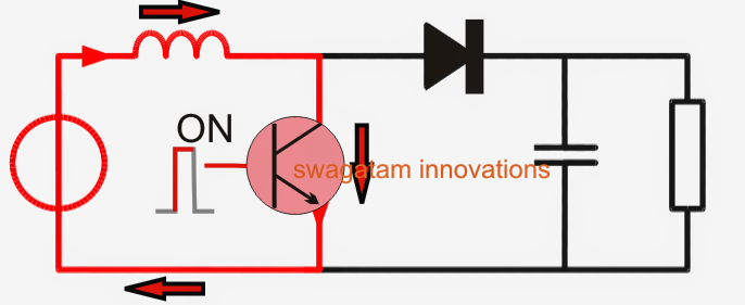
Referring to the following figure, we can see a standard boost converter configuration, the working pattern may be understood as given under:

When the shown device (which could be any standard power BJT or a mosfet) is switched ON, current from the input supply enters the inductor and flows clockwise through the transistor to complete the cycle at the negative end of the input supply.


During the above process the inductor experiences a sudden introduction of current across itself and tries to resist the influx, which results in the storing of some amount of the current in it through the generation of a magnetic field.

At the next subsequent sequence, when the transistor is switched OFF, the conduction of current breaks, yet again forcing a sudden change in the current level across the inductor. The inductor responds to this by kicking back or releasing the stored current. Since the transistor is in the OFF position, this energy finds its path through the diode D and across the shown output terminals in the form of a back EMF voltage.


The inductor performs this by destroying the magnetic field which was earlier created in it while the transistor was in the switch ON mode.

However, the above process of releasing energy is implemented with an opposite polarity, such that the input supply voltage now becomes in series with the inductor back emf voltage. And as we all know that when supply sources join in series their net voltage adds up to produce a bigger combined outcome.

The same happens in a boost converter during the inductor discharge mode, producing an output which may be the combined result of the inductor back EMF voltage and the existing supply voltage, as shown the diagram above

This combined voltage results in a boosted output or a stepped up output which finds its path through the diode D and the across capacitor C to ultimately reach the connected load.

The capacitor C plays quite an important role here, during the inductor discharge mode the capacitor C stores the released combined energy in it, and during the next phase when the transistor switches OFF again and the inductor is in the storing mode, the capacitor C tries to maintain the equilibrium by supplying its own stored energy to the load. See the figure below.


This ensures a relatively steady voltage for the connected load which is able to acquire power during both the ON, and OFF periods of the transistor.

If C is not included then this feature is cancelled resulting in a lower power for the load and lower efficiency rate.


The above explained process continues as the transistor is switched ON/OFF at a given frequency, sustaining the boost conversion effect.

Modes of Operation


A boost converter may be primarily operated in two modes: the continuous mode, and the discontinuous mode.

In continuous mode, the inductor current is never allowed to reach zero during its discharging process (while the transistor is switched OFF).

This happens when the ON/OFF time of the transistor is dimensioned in such a way that the inductor is always connected back quickly with the input supply through the switched ON transistor, before it’s able to get completely discharged across the load and the capacitor C.

This allows the inductor to consistently produce the boost voltage at an efficient rate.

In the discontinuous mode, the transistor switch ON timing may be so wide apart that the inductor may be allowed to get discharged fully and stay inactive in between the switch ON periods of the transistor, creating huge ripple voltages across the load and the capacitor C.

This could make the output less efficient and with more fluctuations.

The best approach is to calculate the ON/OFF time of the transistor which yields maximum stable voltage across the output, meaning we need to make sure that the inductor is optimally switched such that it’s neither switched ON too quickly which might not allow it to discharge optimally, and nor switch it ON very late which might drain it an inefficient point.


Calculating, Inductance, Current, Voltage and Duty Cycle in a Boost Converter


Here we’ll discuss only the continuous mode which is the preferable way to operate a boost converter, let’s evaluate the calculations involved with a boost converter in a continuous mode:

While the transistor is in the switched ON phase, the input source voltage (V_i) is applied across the inductor, inducing a current (I_L) build up through the inductor for a time period, denoted by (t). This may be expressed with the following formula:

ΔIL/Δt = Vt/L

By the time the ON state of the transistor is about to get over, and the transistor is about to switch OFF, the current that is supposed to build up in the inductor may be given by the following formula:


ΔIL(on) = 1/L  0ʃDT   

 or

 Vidt = DT(Vi)/L

Where D is the duty cycle. For understanding its definition you can refer to our previous buck converter related post

L denotes the inductance value of the inductor in Henry.


Now, while the transistor is in the OFF state, and if we assume the diode to be offering minimum voltage drop across it and the capacitor C large enough to be able to produce almost a constant output voltage, then the output current () can be deduced with the help of the following expression

Vi   - Vo  =  LdI/dt

 Also, the current variations () that may occur across the inductor during its discharge period (transistor off state) can be given as:

ΔIL(off) = 1/L x DTʃT    (Vi   - Vo)dt/L = (Vi  - Vo) (1 – D)T / L


Assuming that the converter could be performing with a relatively steady conditions, the magnitude of current or the energy stored inside the inductor throughout the commutation (switching) cycle can be assumed to be steady or at an identical rate, this may be expressed as:


E = ½ L x 2IL


The above also implies that, since the current throughout the commutation period, or at the beginning of the ON state and at the end of the OFF state should be identical, their resultant value of the change in the current level should be a zero, as expressed below:

ΔIL(on)  +  ΔIL(off) = 0


If we substitute the values of  ΔIL(on) and  ΔIL(off) in the above formula from the previous derivations, we get:

ΔIL(on)  -  ΔIL(off) = Vidt/L + (Vi   - Vo) (1 – D)T / L = 0

Further simplifying this yields the following result:
Vo/ Vi = 1 / (1 – D)

or


Vo  = Vi / (1 – D)

The above expression clearly identifies that the output voltage in a boost converter will be always higher than the input supply voltage (across the entire range of the duty cycle, 0 to 1)

Shuffling the terms across the sides in the above equation we get the equation for determining the duty cycle in a boost converter working cycle.
D = 1 –  Vo/ Vi

The above evaluations give us the various formulas for determining the different parameters involved in boost converter operations, which can be effectively used for calculating and optimizing an accurate boost converter design.

Buy LCD LED TV Troubleshooting​ Guide eBook By Imran Ashraf Khan.